


The semiconductor industry has spent decades chasing smaller transistors, squeezing ever more components onto flat silicon wafers until hitting a wall built by the laws of quantum mechanics. But researchers at the University of Illinois Urbana-Champaign have developed a way to stack high-performance silicon circuits directly on top of one another, and their process achieves near-perfect yields at temperatures low enough to finally make monolithic three-dimensional chips practical. This breakthrough could allow chipmakers to increase computing power without shrinking transistors any further, challenging the official story that the industry's only path forward requires exotic new materials or abandoning silicon altogether.
Key points:
- Researchers stacked three layers of silicon circuits with 98 to 100 percent yields.
- The process uses temperatures no higher than 200 degrees Celsius, staying within industry limits.
- Monolithic 3D integration builds each layer directly on top of the previous one, not bonding separate wafers.
- The team used junctionless transistors to avoid high-temperature doping processes.
- Industry partners including IBM, Intel and TSMC are supporting transfer to commercial foundries.
Building upward when shrinking runs out of room
For more than 60 years, Moore's law drove the electronics industry by doubling transistor density on chips every two years. That worked remarkably well until it stopped working. Transistors have become so small that they now approach fundamental limits imposed by atomic dimensions and quantum effects. The contacted gate pitch, a key measure of transistor size, simply is not getting smaller anymore.
Associate professor Qing Cao, who led the research team, put it plainly. "In a sense, we're hitting a limit imposed by physics," he said. "If you look at the actual size of transistors, they're not getting smaller, especially in terms of their contacted gate pitch. This is because we're becoming limited by the intrinsic material properties of silicon and the fundamental rules of quantum mechanics."
The industry has tried workarounds. Some researchers have experimented with two-dimensional materials like molybdenum disulfide. Others have turned to carbon nanotubes or metal oxide semiconductors. But none of those alternatives matched the performance and reliability of standard single-crystalline silicon, the material that has powered computing for half a century.
Cao's team took a different approach. Instead of finding a new material, they found a new way to arrange the old one. They built upward.
The concept is simple. Static random-access memory, which is universal in CPUs and GPUs, currently requires six transistors on a single flat plane to store one bit of information. With vertical integration, those six transistors can be distributed across multiple layers. Cao described the change as replacing a sprawling suburb with high-rises, achieving the same functionality while reducing the spatial footprint and making communication between layers faster and more efficient.
The heat problem that held back an industry
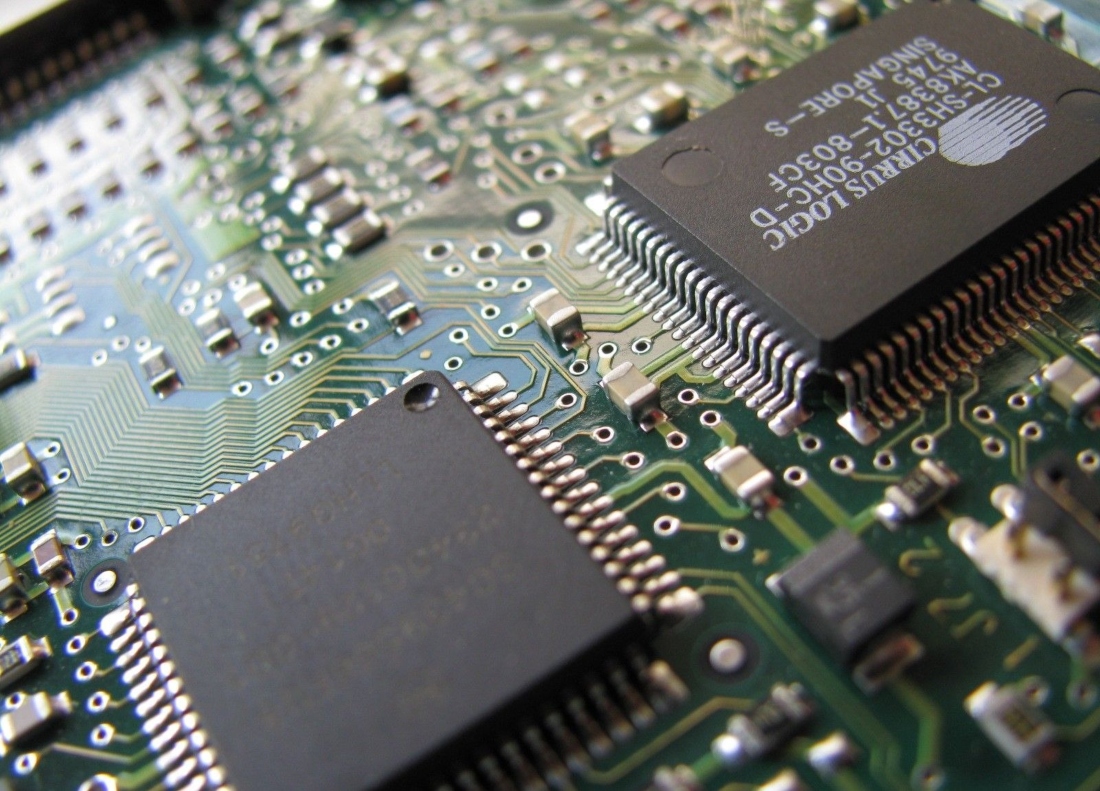
Commercial, three-dimensional chips already exist, but they are not monolithic. Current products like high-bandwidth memory and 3D V-Cache chips are made by fabricating semiconductor devices on separate wafer substrates and then bonding those wafers together. That approach creates relatively large connections between layers and limits how densely components can be integrated. The alignment between layers is coarse, and the vertical connections are large and sparse.
Monolithic three-dimensional integration takes a fundamentally different approach. Each device layer is built directly on top of the previous one during fabrication. This allows 10 to 100 times denser inter-layer vertical connections, smaller separations between layers and precise alignment with nanometer-scale accuracy.
The main barrier was temperature. Forming high-quality crystalline silicon and fabricating high-performance semiconductor devices both require temperatures close to 1,000 degrees Celsius. But once the first layer of circuits and metal wiring is complete, any additional layers must stay below about 400 degrees Celsius to avoid destroying existing structures. This thermal budget constraint has blocked monolithic integration for years.
The Illinois team solved the problem by creating ultrathin, freestanding silicon nano-membranes from a donor wafer and transferring them onto the receiving substrate using a roll laminator. The bonding process requires only 200 degrees Celsius. The membranes are only 10 nanometers thick or less, compared to the 500 to 700 micrometer thickness of a typical wafer. Because they are so thin, these membranes are mechanically flexible and conform to the underlying surface, avoiding the interfacial defects that plague wafer bonding.
The researchers also redesigned transistor fabrication. Conventional transistors require a high-temperature doping process to introduce impurities to the silicon that control its electrical properties. The team used junctionless transistors instead, where the silicon is uniformly and heavily doped before the layering step. Because the films are extremely thin, the gate can still control the channel effectively while the high doping level reduces parasitic contact resistance.
Using this process, the team built three stacked layers containing 625 transistors each. The devices achieved yields between 98 and 100 percent while delivering performance comparable to standard silicon transistors fabricated at much higher temperatures. By connecting the layers with vertical metal lines, the researchers demonstrated three-dimensional integrated logic circuits and static random-access memory cells.
"But most importantly, we've shown that this process is scalable," Cao said. "You can keep stacking layers beyond the three we demonstrated." The researchers are now working to transfer the technology into an industrial semiconductor foundry with support from industry partners including IBM, Intel and TSMC.
The implications for artificial intelligence and data-intensive computing are significant. Vertical integration shortens the needed length of wiring, reducing parasitic capacitance while dramatically increasing the communication bandwidth between devices and circuit blocks. These features offer crucial advantages for applications that demand massive parallel processing.
Sources include:


Please contact us for more information.