


Canadian and Swiss researchers have come up with a new method of making electronic devices for use in the internet of things. Their process leverages 3D printing to produce single-use wireless sensors made from environment-friendly materials that will break down by themselves.

Most electronic devices use plastics, polymers, and other synthetics. These artificial materials last for hundreds of years before they finally decompose. They end up contaminating the environment.
In contrast, the new approach uses cellulose, a natural material derived from wood. Cellulose is biodegradable, making it much more eco-friendly than plastic.
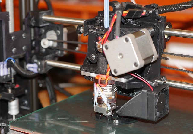
Furthermore, the use of 3D printing techniques allowed them to apply or embed new functions onto shapes and textiles whenever they needed to. The greater flexibility of 3D printers over conventional manufacturing methods led to higher functionality.
"Our eco-friendly 3D printed cellulose sensors can wirelessly transmit data during their life, and then can be disposed [of] without concern of environmental contamination," explained Simon Fraser University (SFU) researcher Woo Soo Kim.
He and his colleagues published their findings in the journal Advanced Electronic Materials. The February issue featured their innovative 3D printing process as the cover story. (Related: Japanese researchers develop a micro-electromechanical energy harvester that runs on ambient energy.)
In pursuit of green electronics
Kim is renowned for his expertise in 3D printed electronics. In addition to leading the research team, he heads SFU's Additive Manufacturing Laboratory and teaches classes at the university's Surrey campus.
His earlier collaboration with his South Korean counterparts at Seoul National University tackled issues in the 3D printing of thin-film transistors. They succeeded in improving the capabilities of 3D printers to manufacture those electronics.
Currently, Kim is running two research projects in collaboration with international partners. One project aims to come up with materials for printable conductive ink in 3D printers. The partners are from Daegu Gyeongbuk Institute of Science and Technology.
The other one is the development of eco-friendly chemical sensors made from cellulose materials. For this project, the SFU researchers receive assistance from Swiss Federal Laboratories for Materials Science (EMPA). Using the advanced 3D printers at the PowerTech Labs in the Surrey campus, they hope to expand the field of green electronics.
"For example, the waste from printed circuit boards is a hazardous source of contamination to the environment," Kim explained. "If we are able to change the plastics in PCB to cellulose composite materials, recycling of metal components on the board could be collected in a much easier way."
New 3D printing technique for chemical sensors made from eco-friendly materials
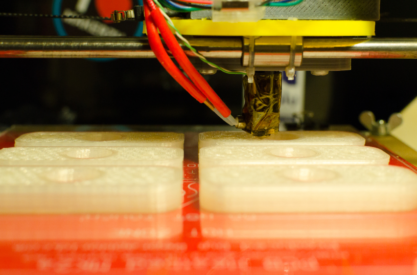
The SFU researchers found their big break in the technology used for the embossing process. Embossing imprinted tiny patterns on the surface of a flexible substrate. The patterns served as electronic circuits.
The substrate was a vital part of an electronic device. For the experiment, the researchers made their substrate from cellulose.
Manufacturers use the embossing process to accurately imprint electronic circuits on the substrate material for a low cost per unit. However, the technology suffers from a couple of problems.
An embossing machine can only imprint the electronic circuits found on its pattern stamp. The stamp needs to be replaced with another one to imprint a different pattern on the substrate. Stamps cost a lot of money. They also take up time to be replaced.
Kim and his colleagues developed a new process technology to address these issues. Their location control system boasts impressive precision. Thanks to this accuracy, the 3D printer can directly imprint patterns on the substrate instead of relying on swapping pattern stamps.
The new approach might change the way manufacturers produce semiconductors for electronic devices like wearable electronics and electronic displays.
Sources include:


Please contact us for more information.